
Like many people these days, I have a home network environment that extends beyond a single modem/router access point. VLAN’s, multiple access points, multiple WAN connections as well as PoE for some smart home devices means that I have a veritable mix of devices at any time sitting on the network. It ocurred to me recently, how long would it take me to replace one of these if it failed? When was the last time I did a configuration backup? …Shit.
Read more...
I’ve recently upgraded 3d printers to a Creality Ender 3 v2 and on the advice of a long time co-conspirator immediately departed down the path of setting up OctoPrint via OctoPi. This is great and I highly recommend it, one button printing without getting out of your chair is addictive. By default OctoPi generates self-signed certificates and allows both secure and insecure connections. We can do better.
Read more...
Controlling temperature is a common requirement for many projects. I’ve been using the ITC308 Wifi controllers for years now due to their low price and have been hopeful for a long while that it would be possible to ditch that …challenging… Inkbird App. The main requirement I had was to be able to programmatically specify the set point (SP) as well as record the current process value (PV), ideally in my existing InfluxDB database. This is that journey…
Read more...I was recently asked to help out with a problematic cluster. The 3 node cluster was running Red Hat Hyperconverged Infrastructure for Virtualization (RHHI-V), essentially a 3 node oVirt cluster running on the same hardware as a 3 node Gluster cluster. Storage is local but shared, as is the compute resources. However, one of the hosts was throwing a “Host (host) cannot access the Storage Domain(s) (storage) attached to the Data Center (dc). Setting Host state to Non-Operational.” and a simple transition via Maintenance mode was not fixing it. This is that story…
Read more...
I've been looking for a "light weight" method of getting aggregated logging across the home lab for a while. Loki has been interesting since its release, so I decided to have a play with it. I've been using Grafana heavily for years, so it seemed like the logical choice, as it is much lower on resources than Graylog, the other platform I was investigating.
Read more...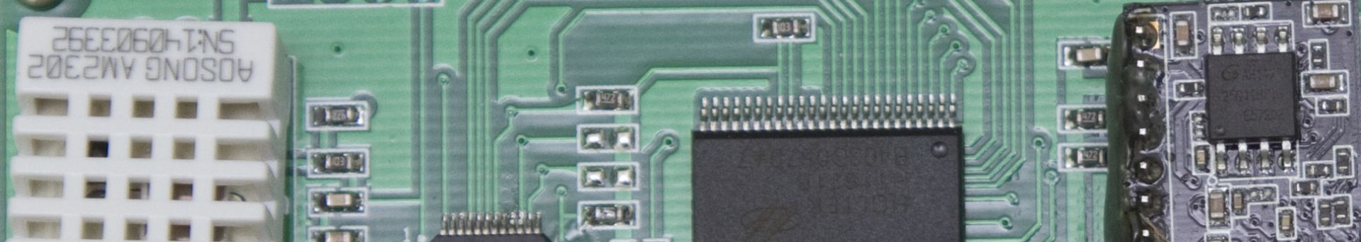
Reverse engineering the USR-HTW Temperature and Humidity Sensor.
Read more...
The construction and testing of a helical antenna for 1420MHz.
Read more...
Yesterday was the transit of Venus here on Earth. If you haven’t already heard about it, then you for sure you don’t know the people I know!
Read more...So, I have finally gotten around to writing something again! I have recently been working on a board that is using an FTDI FT2232H as the interface between an FPGA and USB interface. The requirement is simple, get data from FPGA to USB as fast as possible. I have encountered some problems getting the FTDI chip to work properly in this mode.
Read more...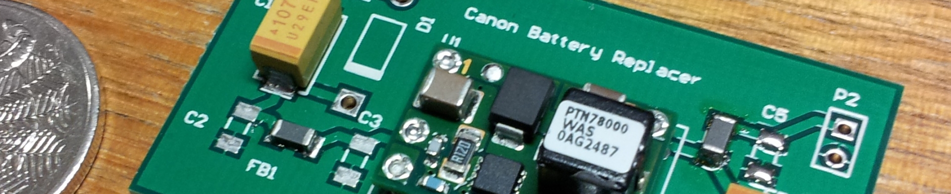
One of my other hobbies is photography, and whilst I don’t spend as much time with the camera as I would like I still like to have plenty of power. I shoot with a 30D and/or 40D, which uses the old style BP-511/A Canon battery. The dilemna I had is that I would like to power my camera from a 12-14V source (such as a SLA battery) to get plenty of juice, but I need to provide the requisite 7.4V expected from the battery.
Read more...
One of the projects that I am tinkering with at the moment is the creation of an audio capture device that can be phase locked to an external reference. The primary reason for this is not chasing extremely high quality audio – the contrary in fact, I don’t particularly care for the audio quality.
Read more...
My new PCB has just been mated with a S3E500 starter kit for the first time. They look quite good together I reckon?
Read more...
Something that a mate and I had seen on the internet before, but never tried – the formation of plasma in a microwave. From a grape!
Read more...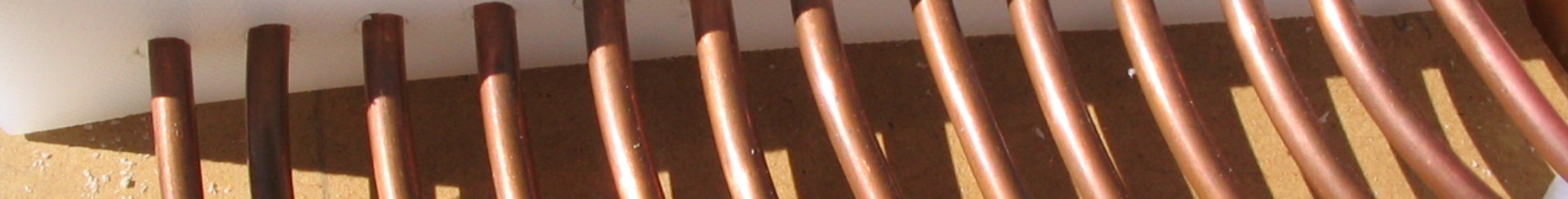
The construction of my first tesla coil, started in 2003.
Read more...